- 您现在的位置:买卖IC网 > Sheet目录334 > ISL6597CRZ (Intersil)IC MOSFET DRVR DUAL SYNC 16-QFN
�� �
�
�ISL6597�
�PVCC�
�R� HI1�
�BOOT�
�G�
�C� GD�
�D�
�C� DS�
�overcharging,� exceeding� the� device� rating.� Low-profile�
�MOSFETs,� such� as� Direct� FETs� and� multi-SOURCE� leads�
�devices� (SO-8,� LFPAK,� PowerPAK),� have� low� parasitic� lead�
�inductances� and� are� preferred.�
�Layout� Considerations�
�R� LO1�
�UGATE�
�R� G1�
�R� GI1�
�C� GS�
�Q1�
�A� good� layout� helps� reduce� the� ringing� on� the� switching�
�node� (PHASE)� and� significantly� lower� the� stress� applied� to�
�S�
�PHASE�
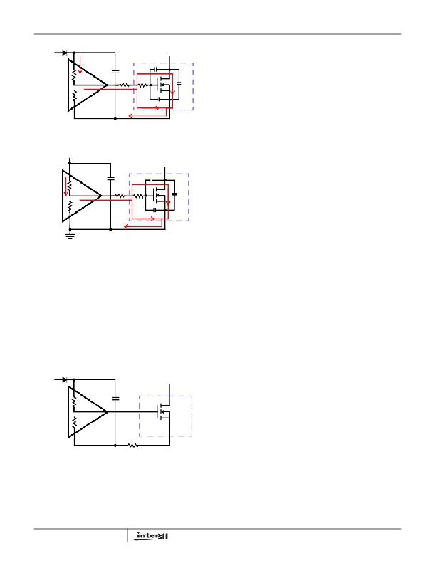
�FIGURE� 3.� TYPICAL� UPPER-GATE� DRIVE� TURN-ON� PATH�
�PVCC�
�D�
�C� GD�
�the� output� drives.� The� following� advice� is� meant� to� lead� to� an�
�optimized� layout� and� performance:�
�?� Keep� decoupling� loops� (VCC-GND,� PVCC-PGND� and�
�BOOT-PHASE)� short� and� wide,� at� least� 25� mils.� Avoid�
�using� vias� on� decoupling� components� other� than� their�
�ground� terminals,� which� should� be� on� a� copper� plane� with�
�at� least� two� vias.�
�?� Minimize� trace� inductance,� especially� on� low-impedance�
�R� HI2�
�LGATE�
�G�
�C� DS�
�lines.� All� power� traces� (UGATE,� PHASE,� LGATE,� PGND,�
�PVCC,� VCC,� GND)� should� be� short� and� wide,� at� least� 25�
�R� LO2�
�GND�
�R� G2�
�R� GI2�
�C� GS�
�S�
�Q2�
�mils.� Try� to� place� power� traces� on� a� single� layer,�
�otherwise,� two� vias� on� interconnection� are� preferred�
�where� possible.� For� no� connection� (NC)� pins� on� the� QFN�
�part,� connect� it� to� the� adjacent� net� (LGATE2/PHASE2)� can�
�reduce� trace� inductance.�
�FIGURE� 4.� TYPICAL� LOWER-GATE� DRIVE� TURN-ON� PATH�
�Application� Information�
�MOSFET� Selection�
�The� parasitic� inductances� of� the� PCB� and� of� the� power�
�devices’� packaging� (both� upper� and� lower� MOSFETs)� can�
�cause� serious� ringing,� exceeding� absolute� maximum� rating�
�of� the� devices.� The� negative� ringing� at� the� edges� of� the�
�PHASE� node� could� increase� the� bootstrap� capacitor� voltage�
�through� the� internal� bootstrap� diode,� and� in� some� cases,� it�
�may� overstress� the� upper� MOSFET� driver.� Careful� layout,�
�proper� selection� of� MOSFETs� and� packaging� can� go� a� long�
�way� toward� minimizing� such� unwanted� stress.�
�?� Shorten� all� gate� drive� loops� (UGATE-PHASE� and� LGATE-�
�PGND)� and� route� them� closely� spaced.�
�?� Minimize� the� inductance� of� the� PHASE� node.� Ideally,� the�
�source� of� the� upper� and� the� drain� of� the� lower� MOSFET�
�should� be� as� close� as� thermally� allowable.�
�?� Minimize� the� current� loop� of� the� output� and� input� power�
�trains.� Short� the� source� connection� of� the� lower� MOSFET�
�to� ground� as� close� to� the� transistor� pin� as� feasible.� Input�
�capacitors� (especially� ceramic� decoupling)� should� be�
�placed� as� close� to� the� drain� of� upper� and� source� of� lower�
�MOSFETs� as� possible.�
�?� Avoid� routing� relatively� high� impedance� nodes� (such� as�
�PWM� and� ENABLE� lines)� close� to� high� dV/dt� UGATE� and�
�PHASE� nodes.�
�PVCC�
�BOOT�
�D�
�In� addition,� connecting� the� thermal� pad� of� the� QFN� package�
�to� the� power� ground� through� multiple� vias� is� recommended.�
�This� is� to� improve� heat� dissipation� and� allow� the� part� to�
�achieve� its� full� thermal� potential.�
�R� HI1�
�R� LO1�
�UGATE�
�G�
�Q1�
�Upper� MOSFET� Self� Turn-On� Effects� At� Startup�
�Should� the� driver� have� insufficient� bias� voltage� applied,� its�
�outputs� are� floating.� If� the� input� bus� is� energized� at� a� high�
�R� PH� =� 1� Ω� to� 2� Ω�
�S�
�PHASE�
�FIGURE� 5.� PHASE� RESISTOR� TO� MINIMIZE� SERIOUS�
�NEGATIVE� PHASE� SPIKE�
�The� D� 2� -PAK,� or� D-PAK� packaged� MOSFETs,� have� large�
�parasitic� lead� inductances� and� are� not� recommended� unless�
�a� phase� resistor� (R� PH� ),� as� shown� in� Figure� 5,� is�
�implemented� to� prevent� the� bootstrap� capacitor� from�
�8�
�dV/dt� rate� while� the� driver� outputs� are� floating,� due� to� the�
�self-coupling� via� the� internal� C� GD� of� the� MOSFET,� the�
�UGATE� could� momentarily� rise� up� to� a� level� greater� than� the�
�threshold� voltage� of� the� MOSFET.� This� could� potentially� turn�
�on� the� upper� switch� and� result� in� damaging� inrush� energy.�
�Therefore,� if� such� a� situation� (when� input� bus� powered� up�
�before� the� bias� of� the� controller� and� driver� is� ready)� could�
�conceivably� be� encountered,� it� is� a� common� practice� to�
�place� a� resistor� (R� UGPH� )� across� the� gate� and� source� of� the�
�FN9165.1�
�May� 4,� 2007�
�发布紧急采购,3分钟左右您将得到回复。
相关PDF资料
ISL6605IBZ
IC DRIVER MOSFET DUAL SYNC 8SOIC
ISL6608IR-T
IC MOSFET DRVR SYNC BUCK 8-QFN
ISL6609AIRZ-TK
IC MOSFET DVR SYNC RECT 8-QFN
ISL6610IRZ
IC MOSFET DRVR DUAL SYNC 16-QFN
ISL6612ACBZ
IC DRIVER MOSFET SYNC BUCK 8SOIC
ISL6612BCBZ
IC DRIVER MOSFET SYNC BUCK 8SOIC
ISL6613IR-T
IC MOSFET DRVR SYNC BUCK 10-DFN
ISL6614AIR-T
IC DRIVER DUAL SYNC BUCK 16-QFN
相关代理商/技术参数
ISL6597CRZ-T
功能描述:IC MOSFET DRVR DUAL SYNC 16-QFN RoHS:是 类别:集成电路 (IC) >> PMIC - MOSFET,电桥驱动器 - 外部开关 系列:- 标准包装:50 系列:- 配置:高端 输入类型:非反相 延迟时间:200ns 电流 - 峰:250mA 配置数:1 输出数:1 高端电压 - 最大(自引导启动):600V 电源电压:12 V ~ 20 V 工作温度:-40°C ~ 125°C 安装类型:通孔 封装/外壳:8-DIP(0.300",7.62mm) 供应商设备封装:8-DIP 包装:管件 其它名称:*IR2127
ISL6598DRZ-T
制造商:Intersil Corporation 功能描述:PB-FREE 48LD 7X7 QFN, T&R, GRAPHICS PROCESSOR DIGITAL CONT. - Tape and Reel 制造商:Intersil Corporation 功能描述:IC GRAPHICS PROCESSOR DGTL 制造商:Intersil 功能描述:4 8LD 7X7 GRAPHICS PROCESSOR DIGTL CONT
ISL6605CB
功能描述:IC MOSFET DRVR SYNC BUCK 8-SOIC RoHS:否 类别:集成电路 (IC) >> PMIC - MOSFET,电桥驱动器 - 外部开关 系列:- 标准包装:50 系列:- 配置:低端 输入类型:非反相 延迟时间:40ns 电流 - 峰:9A 配置数:1 输出数:1 高端电压 - 最大(自引导启动):- 电源电压:4.5 V ~ 35 V 工作温度:-40°C ~ 125°C 安装类型:表面贴装 封装/外壳:TO-263-6,D²Pak(5 引线+接片),TO-263BA 供应商设备封装:TO-263 包装:管件
ISL6605CB-T
功能描述:IC MOSFET DRVR SYNC BUCK 8-SOIC RoHS:否 类别:集成电路 (IC) >> PMIC - MOSFET,电桥驱动器 - 外部开关 系列:- 标准包装:50 系列:- 配置:低端 输入类型:非反相 延迟时间:40ns 电流 - 峰:9A 配置数:1 输出数:1 高端电压 - 最大(自引导启动):- 电源电压:4.5 V ~ 35 V 工作温度:-40°C ~ 125°C 安装类型:表面贴装 封装/外壳:TO-263-6,D²Pak(5 引线+接片),TO-263BA 供应商设备封装:TO-263 包装:管件
ISL6605CB-TS2495
制造商:Rochester Electronics LLC 功能描述: 制造商:Intersil Corporation 功能描述:4 A HALF BRDG BASED MOSFET DRIVER, 8 Pin Plastic SOP
ISL6605CBZ
功能描述:功率驱动器IC VER OF ISL6605CB RoHS:否 制造商:Micrel 产品:MOSFET Gate Drivers 类型:Low Cost High or Low Side MOSFET Driver 上升时间: 下降时间: 电源电压-最大:30 V 电源电压-最小:2.75 V 电源电流: 最大功率耗散: 最大工作温度:+ 85 C 安装风格:SMD/SMT 封装 / 箱体:SOIC-8 封装:Tube
ISL6605CBZ
制造商:Intersil Corporation 功能描述:MOSFET Driver IC
ISL6605CBZA
功能描述:IC MOSFET DRVR SYNC BUCK 8-SOIC RoHS:是 类别:集成电路 (IC) >> PMIC - MOSFET,电桥驱动器 - 外部开关 系列:- 标准包装:6,000 系列:*